A new study by a collaborative team from the University of Twente and the e-Science Centre in Amsterdam has made a significant leap in the field of nanotechnology. Their research compared the transmission of light through a utopian model with a real 3D nanostructure. These nanostructures are integral to our daily technology such as smartphones and solar panels.
The team’s innovative approach uses the real 3D nanostructure itself, obtained through precise X-ray imaging, as input for their optical study. This way, the researchers could directly compare the real nanostructure with an idealised or ‘utopian’ model. The findings reveal that, unlike the ideal design, the real nanostructure exhibits a strong confinement of light which is completely absent in the utopian design.
Chip predictability
Device predictability is crucial for applications ranging from metrology for chip fabrication, and smart lighting with light-emitting diodes, to atmosphere observations with nanosatellites. However, no matter how expensive and well-equipped the facility, inevitable deviations appear during nanofabrication. Two consecutively made nanostructures are never exactly the same down to the level of the placement of the atoms since, for example, fabrication equipment slowly varies in time. Ultimately, even if all equipment works perfectly, entropy and chaos forbid exact copies to be made, making devices less predictable.
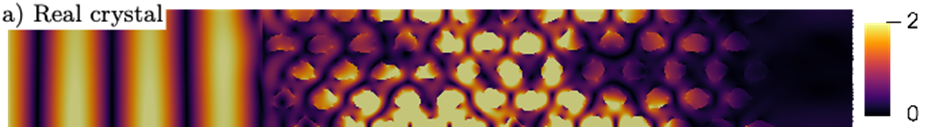
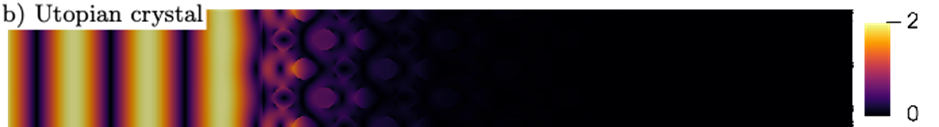
Figure 1. Light distribution (E-field) in a) the real crystal and b) utopian crystal. Lighter colours correspond to brighter light. Bright light is confined inside the real crystal, but absent in the utopian model.
New device functionalities
The Twente-Amsterdam team’s research not only enhances our understanding of these deviations but also opens the door to new device functionalities. Vos explains: “There are major differences between the real and the utopian structure. For example, where the utopian structure forbids light from entering, the real structure holds a high energy density of light (see figure 1). The real light distribution has a peculiar pattern that light is prevented from exiting to the right, as originally designed. The intense and confined light may even be used for completely new functions, such as an optical switch or a sensor!”
The Team
The research was done by Lars Corbijn van Willenswaard, Stef Smeets, Nicolas Renaud, Matthias Schlottbom, Jaap van der Vegt, and Willem Vos from the University of Twente. Lars is a PhD student in the COPS and MACS chairs, Stef and Nicolas are staff members of the NWO e-Science Centre in Amsterdam, Matthias is an associate professor and Jaap professor (emeritus) of MACS, and Willem professor of COPS.
The research was funded by NWO JCSER Program, project 680-91-084, “Accurate and Efficient Computation of the Optical Properties of Nanostructures for Improved Photovoltaics”, by NWO (FOM) program nr. 138 “Stirring of light!”, and by NWO-TTW program P15-36 “Free-Form Scattering Optics” (FFSO).
The paper
The paper entitled “Non-utopian optical properties computed of a tomographically reconstructed real photonic band gap crystal” appears in Optics Express that is published by the professional society Optica (previously the Optical Society of America (OSA)). The paper is available online.
DOI: 10.1364/OE.519464


